Nagasaki Univ. Plasma Engineering Laboratory

Under construction
Sputter-deposition of ZnO based transparent conductive thin films
 ZnO based transparent conductive oxide (TCO) is a promissing candidate to replace tin doped indium oxide (ITO) that has been widely used.
ZnO has disadvantages in inherent conductivity compared with ITO, but has advantages over ITO in safety and resource cost.
Key issues to improve the conductivity of TCO films are the use of metal doping and the control of a thin buffer layer between substrate and TCO layer.
Our ultimate goal is to deposit high quality ZnO-TCO films at room temeratures on the large area plastic sheet substrates as well as glass or silicon substrates, with good spatial uniformity and high deposition rate.
 We are doing researches on metal-doped ZnO by using different sputtering apparatus;
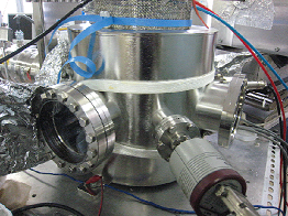
one is a conventional DC or RF planar magnetron sputtering (DCMS, RFMS: left top) apparatus,
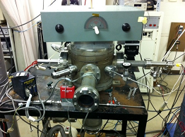
and the other is an inductively-coupled-plasma assisted DC sputtering (ICP assisted DCMS: left bottom) apparatus.
In DCMS or RFMS, conductivity of the deposited film becomes nonuniform over the substrate.
The films deposited at the substrate position just facing the target eroded area are heavily bombarded by energetic oxygen negative ions
and charge-exchanged neutral atoms. Thus, both carrier density and mobility are decreased there.
One way to reduce this harmful energetic negative ion bombardment is using off-axis substrate arrangement.
Another way is to employ "ICP assisted DCMS". Since the ICP assisted DCMS is operated with much lower target voltage at much higher pressure than RFMS,
the energetic negative ion bombardment is much less, resulting in more uniform spatial quality profile.
The problem of high density "ICP assisted DCMS" is the excess substrate heating compared with RFMS.
In this research, measurements of particle and energy fluxes onto the substrate are very important,
and the effect of implimented thin buffer layer needs more investigation.
Development of plasma diagnostics and applications to plasma processes
 We use variety of plasma diagnostics from probe measurements to optical measurements such as optical emission spectroscopy, laser absorption, laser induced fluorescence, laser photodetachment, etc.
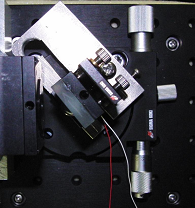
Good quality and cheap diode laser is available in these days. Recently we have made external cavity diode lasers (ECDL) and have been using it as a light source of tunable diode laser absorption spectroscopy. By using this system, velocity distributions of neutral and ionic species are under investigation. The left photograph shows the home-made Littrow ECDL.
Sputter-deposition of magnetic fikms
Development of Nd-Fe-B permanent magnetic film is attractive for future MEMS application. Our aim is to develop high performance permanent magnetic film with multi-layer structure. Preliminary experiments on Nd-Fe-B/Ta bi-layer structure showed promissing results.
※This research project is a collaboration with Profs Fukunaga and Nakano of Nagasaki Univ.